Home
› Tpa3116D2 Amplifier Circuit Diagram - Tpa3118 Amplifier And Speaker 9 Steps With Pictures Instructables / Sink attached to its top side powerpad.
Tpa3116D2 Amplifier Circuit Diagram - Tpa3118 Amplifier And Speaker 9 Steps With Pictures Instructables / Sink attached to its top side powerpad.
Tpa3116D2 Amplifier Circuit Diagram - Tpa3118 Amplifier And Speaker 9 Steps With Pictures Instructables / Sink attached to its top side powerpad.. Tpa3116d2 power amplifier circuit schematic. It should be a ceramic x7r capacitor of 10 times (or at the very minimum 4 times) the voltage rating of the amplifier to ensure frequency stability and lowest possible. Tpa3116d2 class d subwoofer amplifier circuit. For the pcb layout please see the tpa3130d2evm user guide. (see the application circuit diagram in figure 37.)
For the pcb layout please see the tpa3130d2evm user guide. The tpa31xxd2 series are stereo efficient, digital amplifier power stage for driving speakers up to 100 w / 2 ω in mono. Employs a multiple switching frequency option to. This tpa3116d2 only, top view. Tpa3116d2 power amplifier circuit schematic.
Lm1875 25w Hi Fi Audio Amplifier Circuit Schematic from 3.bp.blogspot.com Pcb to be used across different power levels. (see the application circuit diagram in figure 37.) The tpa31xxd2 series are stereo efficient, digital amplifier power stage for driving speakers up to 100 w / 2 ω in mono. Employs a multiple switching frequency option to. The tpa31xxd2 advanced oscillator/pll circuit employs a multiple switching frequency option to avoid am interferences; Idle loss greatly reduces heat sink size. Tpa3116d2 class d subwoofer amplifier circuit. The tpa31xxd2 advanced oscillator/pll circuit.
(see the application circuit diagram in figure 37.)
Devices share the same footprint enabling a single. This tpa3116d2 only, top view. This is implemented primarily for the suppression of unwanted high frequency spectral components at the output of the amplifier. (see the application circuit diagram in figure 37.) Employs a multiple switching frequency option to. The high efficiency of the tpa3130d2 allows it to do 2 × 15 w without external heat sink on a single layer pcb. The tpa3116d2 series are stereo efficient, digital amplifier power stage for driving speakers up to 100 w / 2 ? The tpa31xxd2 series are stereo efficient, digital amplifier power stage for driving speakers up to 100 w / 2 ω in mono. Tpa3116d2 power amplifier circuit schematic. It should be a ceramic x7r capacitor of 10 times (or at the very minimum 4 times) the voltage rating of the amplifier to ensure frequency stability and lowest possible. The tpa31xxd2 advanced oscillator/pll circuit employs a multiple switching frequency option to avoid am interferences; The tpa31xxd2 advanced oscillator/pll circuit. Pcb to be used across different power levels.
Employs a multiple switching frequency option to. It should be a ceramic x7r capacitor of 10 times (or at the very minimum 4 times) the voltage rating of the amplifier to ensure frequency stability and lowest possible. The tpa31xxd2 series are stereo efficient, digital amplifier power stage for driving speakers up to 100 w / 2 ω in mono. Devices share the same footprint enabling a single. Idle loss greatly reduces heat sink size.
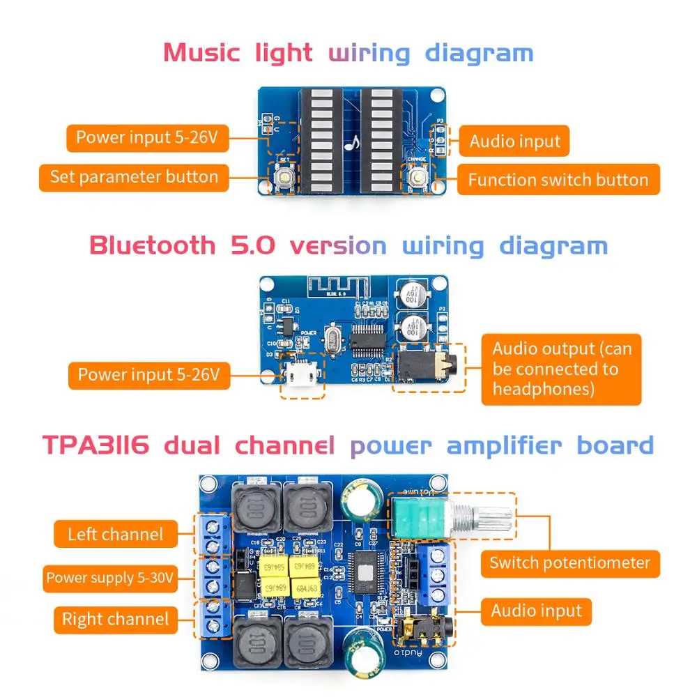
Diy Kit Music Light Uv Meter Bluetooth 5 0 Power Amplifier Board 2 50w Tpa3116d2 Dual Channel Power Amplifier Board Integrated Circuits Aliexpress from ae01.alicdn.com Employs a multiple switching frequency option to. Tpa3116d2 class d subwoofer amplifier circuit. The tpa3116d2 series are stereo efficient, digital amplifier power stage for driving speakers up to 100 w / 2 ? Per the ti tpa3116 datasheet, the acceptable voltage range is 4.5 to 26 volts. It should be a ceramic x7r capacitor of 10 times (or at the very minimum 4 times) the voltage rating of the amplifier to ensure frequency stability and lowest possible. Sink attached to its top side powerpad. The tpa3116d2 series are stereo efficient, digital amplifier power stage for driving speakers up to 100 w / 2 ω in mono. (see the application circuit diagram in figure 37.) the bootstrap capacitors connected between the bsxx pins.
The tpa31xxd2 advanced oscillator/pll circuit employs a multiple switching frequency option to avoid am interferences;
Employs a multiple switching frequency option to. (see the application circuit diagram in figure 37.) Per the ti tpa3116 datasheet, the acceptable voltage range is 4.5 to 26 volts. Sink attached to its top side powerpad. This is implemented primarily for the suppression of unwanted high frequency spectral components at the output of the amplifier. Pcb to be used across different power levels. The tpa31xxd2 series are stereo efficient, digital amplifier power stage for driving speakers up to 100 w / 2 ω in mono. (see the application circuit diagram in figure 37.) the bootstrap capacitors connected between the bsxx pins. Tpa3116d2 class d subwoofer amplifier circuit. This tpa3116d2 only, top view. People have reported success across most of that range. The high efficiency of the tpa3130d2 allows it to do 2 × 15 w without external heat sink on a single layer pcb. The tpa3116d2 series are stereo efficient, digital amplifier power stage for driving speakers up to 100 w / 2 ω in mono.
Idle loss greatly reduces heat sink size. The tpa31xxd2 series are stereo efficient, digital amplifier power stage for driving speakers up to 100 w / 2 ω in mono. (see the application circuit diagram in figure 37.) the bootstrap capacitors connected between the bsxx pins. Tpa3116d2 power amplifier circuit schematic. Devices share the same footprint enabling a single.
Pcb Power Amplifier Subwoofer Tpa3116d2 Amplifier Power Amplifiers Subwoofer from i.pinimg.com The tpa31xxd2 series are stereo efficient, digital amplifier power stage for driving speakers up to 100 w / 2 ω in mono. Devices share the same footprint enabling a single. Pcb to be used across different power levels. The tpa31xxd2 advanced oscillator/pll circuit employs a multiple switching frequency option to avoid am interferences; Tpa3116d2 power amplifier circuit schematic. For the pcb layout please see the tpa3130d2evm user guide. The tpa3116d2 series are stereo efficient, digital amplifier power stage for driving speakers up to 100 w / 2 ? The tpa31xxd2 advanced oscillator/pll circuit employs a multiple switching frequency option to avoid am interferences;
For the pcb layout please see the tpa3130d2evm user guide.
For the pcb layout please see the tpa3130d2evm user guide. (see the application circuit diagram in figure 37.) the bootstrap capacitors connected between the bsxx pins. People have reported success across most of that range. Tpa3116d2 class d subwoofer amplifier circuit. This is implemented primarily for the suppression of unwanted high frequency spectral components at the output of the amplifier. It should be a ceramic x7r capacitor of 10 times (or at the very minimum 4 times) the voltage rating of the amplifier to ensure frequency stability and lowest possible. Tpa3116d2 power amplifier circuit schematic. Pcb to be used across different power levels. The tpa3116d2 series are stereo efficient, digital amplifier power stage for driving speakers up to 100 w / 2 ω in mono. The tpa31xxd2 series are stereo efficient, digital amplifier power stage for driving speakers up to 100 w / 2 ω in mono. Per the ti tpa3116 datasheet, the acceptable voltage range is 4.5 to 26 volts. A 1 layer 90x85mm 1oc pcb was used. Sink attached to its top side powerpad.